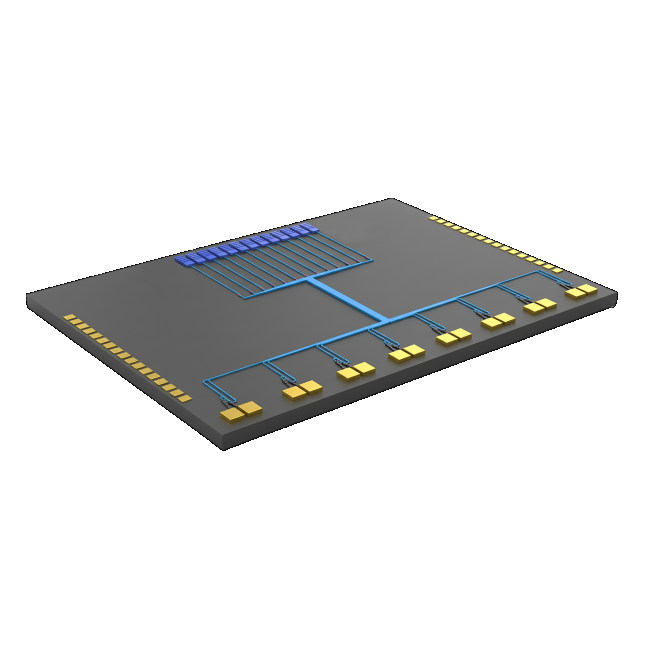
3.2T-DR8 Transmitter PIC
RR4-C145 and RR8-C145 O/C Band Ring Resonator Modulator
This modulator is delivering unprecedented bandwidth making them an undisputed option to implement high-performance transceivers. Together with an optimized driver they are providing substantial contributions to reduce system power dissipation and enhancing signal integrity. In conclusion, its compact, efficient design is enabling seamless integration and scalability.
Key Features
-
 400G per lane generation
 -

3-dB electro-optic bandwidth >145 GHz
-

Lumped, low-capacitance RF design
-

O/C band operation
-

4/8-channel device
-
 Insertion loss (static) below 5 dB (fiber to fiber)
Description
This component is an advanced multi-channel ring resonator modulator designed for high-speed optical communication applications. Available for both O band (1310 nm) and C band (1550 nm), this modulator presents a 3-dB electro-optical bandwidth exceeding 145 GHz, therefore it is a key enabler for next-generation transceivers and data transmission at 200+ GBaud PAM4.
Moreover, with a lumped, low-capacitance design, it provides superior RF performance and higher optical signal integrity as a result. With an attractive static insertion loss, it ensures a high system power efficiency by wasting less laser power. In addition, the extinction ratio and the optical modulation amplitude deliver excellent, standard complying operation.
Low Drive Voltage
Ring resonators modulators do not have a definition for half-wave voltage (Vπ), instead Vdrive is specified. From a 50 Ω driver just 1 Vpp is required, from a high-impedance driver the optimal input is 2 Vpp differential signal for highest performance. This is industry leading for this type of device.
Related Papers
Reliability
Telcordia GR-468 qualification is the target and the achievement will be announced in due time. The current status is released to engaging customers.
We encapsulate our devices at wafer lavel and track all metrics in real-time including the operating point, peak wavelength, insertion loss, extinction ratio and more.
Driver Co-design
The modulator can be drived with low and high-impedance driver. For best performance, we suggest shortest bond wires and RF properties, In addition, a dedicated high-Z compatible device with optimized pad layout. In conclusion, a Driver and modulator co-design generally optimizes system performance.
Operating Point Tuning
Each plasmonic ring can be tuned with a thermo-optic phase shifter in order to set the operating point for best ER and OMA trade-off. Further these elements are also used to compensate for drifts due to temperature changes or laser drifts.
Resonance tuning range is covers the full free spectral range with an external controller.
Advanced variants of this component also include an efficient 1:100 tap and a monitoring photo-diode.
Operation Point Stability
Plasmonic modulators present a much lower wavelength shift due to temperature changes compared to SiPh MRMs (M. Eppenberger, et al. Resonant plasmonic micro-racetrack modulators with high bandwidth and high temperature tolerance (Nature Photonics, 2023)). For instance, typical measured drifts are in range of 0.02 nm/K.
Variants and Specifications
Polariton offers this device in various variants, being single, quad and octo channel, ideal for a wide range of optical interconnect solutions.
| EO bandwidth | Optical band | Channels | RR variant | Ordering code |
| 145 GHz | O band | 4 | differential | RR4-C145-o |
| 145 GHz | C band | 4 | differential (1) | RR4-C145-c |
| 145 GHz | O band | 4 | differential, monitoring PD, grating couplers | RR4-C145-opg |
| 145 GHz | O band | 4 | differential, monitoring PD, edge couplers | RR4-C145-ope |
| 145 GHz | O band | 8 | differential, monitoring PD, grating couplers | RR8-C145-opg |
| 145 GHz | O band | 8 | differential, monitoring PD, edge couplers | RR8-C145-ope |
(1) In addition, a probable 4-channel version with GSG probes for GS operation is available on demand.
Performance Specifications
| O band | C band | |
| Peak wavelength | 1310 nm | 1550 nm |
| Static Insertion loss, fiber to fiber (IL) | <5 dB | <5 dB |
| Static extinction ratio (ER) | >8 dB | >8 dB |
| 3-dB EO bandwidth | >145 GHz | >145 GHz |
| Vdrive @ 100 kHz, @ High-Z driver | <2 Vppd | <2 Vppd |
| DC bias (operating point tuning) voltage | <1.5 V | <1.5 V |
| Free Spectral Range | ~4.7 nm | ~4.7 nm |
Maximum Ratings
| O band | C band | |
| Optical input power** | 19 dBm | 19 dBm |
| RF input power @ 50 Ohm | 18 dBm | 18 dBm |
| DC voltage at RF input | 0 V | 0 V |
| DC bias voltage DC bias current | 2.5 V 15 mA | 2.5 V 15 mA |
| Operating / storage temperature | 0°C to 85°C | 0°C to 85°C |
* Plasmonic modulators are high-impedance devices. Twice the voltage provided by a 50-Ohm signal source will drop across the plasmonic modulator. Using a DC source or a high-impedance-matched driver, double the voltage is required to switch the modulator from the on to the off state.
** Input power for 4 parallel RRM channels. Operation time of 8000 h at 85°C with a Vπ degradation <10%.
Mechanical and Optical Specifications
| O band | C band | |
| Grating couplers (input and output) | Grating coupler (GC), 127 um pitch | Grating coupler (GC), 127 um pitch |
| Edge couplers (input and output) | tba | tba |
| Typical center wavelength at GC angle | 1310 nm at 8° | 1550 nm at 8° |
| Optical source needed | DFB laser 1310 nm | DFB laser 1550 nm |
| Electrical RF and DC interface | Uniform pitch 100 μm (pad layout see drawing) | Uniform pitch 100 μm (pad layout see drawing) |


