Photonic Integrated Circuits
What is a PIC and what are the challenges today?

Visualization of a monolithic PIC. In a PIC photonic building blocks (having a photonic function) are connected with optical waveguides to form more complex functions.
A photonic integrated circuit (PIC) is a chip that performs optical signal processing. Consequently, for communications, sensing, automotive and computing, PICs are central to the current and future applications. Just as it is possible to produce a chip with millions of transistors on it, it is possible to produce a chip with thousands of photonic devices to control and manipulate light. Indeed, as the digital transformation impacts more and more sectors, the demand for PICs will increase.
The evolution of PICs has been closely related to materials and their optical characteristics. Such materials give origin to so called platforms. The differentiation comprises capabilities like the optical power, the optical losses, the possibility to build efficient lasers or fast modulators, and several others more.
The PIC industry is in front of a couple of challenges:
- The diffraction limit of light is blocking the miniaturization of photonic components to the nanoscale
- The demand of PICs is increasing and not all material platforms provide enough capacity to scale
- The switching speed of components is increasing
- Most PICs do not provide a good profitability as a proof that the industry is still in its infancy. Government and venture funding is essential.
- Emerging photonic applications will push for evolution. We expect 6G, automotive LiDAR, consumer healthcare, artificial intelligence (AI), optical computing, virtual reality (VR) and augmented reality (AR) to have a relevant transformation potential.
Silicon Photonics Addresses Scaling
Silicon photonics is compatible to CMOS processing and can be manufactured with semiconductor process lines. In particular it can profit from current 200 and 300 mm wafer processing technologies, and a virtually unlimited semiconductor supply chain.
Silicon is transparent above 1100 nm making it a key technology for communication that has traditionally been in the infrared region between 1300 and 1700 nm. Today the most typical bands for optical communication are the O band (1260 … 1360 nm) and the C band (1530 … 1565 nm).
The compatibility to CMOS further enables monolithic integration with logic for medium complexity processing tasks, excluding maybe the high-end processing that targets sub 10 nm process nodes anyway.
Large Global Players
Many large and small semiconductor companies have released PDKs for silicon photonics providing a wealth of options for fabless operation, namely:
- Global Foundries, Fotonix process offering monolithic integration with CMOS and RF CMOS, 300mm high-volume manufacturing,
- AMF Silicon on Insulator (SOI) and Silicon Nitride on SOI platforms,
- Imec & Silterra 200 mm and 300 mm silicon photonics process, supporting through-silicon vias (TSV), microbumps, and embedded microbumps,
- Tower Semiconductors offers silicon photonics on 200 mm wafers,
- and many more.
Silicon Needs New Modulator Technologies
Silicon electro-absorption modulators are coming to the end of their technology lifespan, limited by the diffraction limit of light and maximum modulation speed. New technology is required. Polariton masters plasmonics, which is actually based on different physics, and exploits different optical effects. Fortunately light can be easily converted into plasmons and back with moderate losses. This results in the technology that brings silicon photonics into the 2030s for optical communication.
Plasmonics Platform Specifications
- Maximum demonstrated EO bandwidth: 1 THz
- Maximal practical frequency today (2025): 220 GHz
- Phase shifter dimensions: 5-25 um (length), 50-250 nm (width)
- 0.5 pJ/bit (including power dissipated by driver circuit)


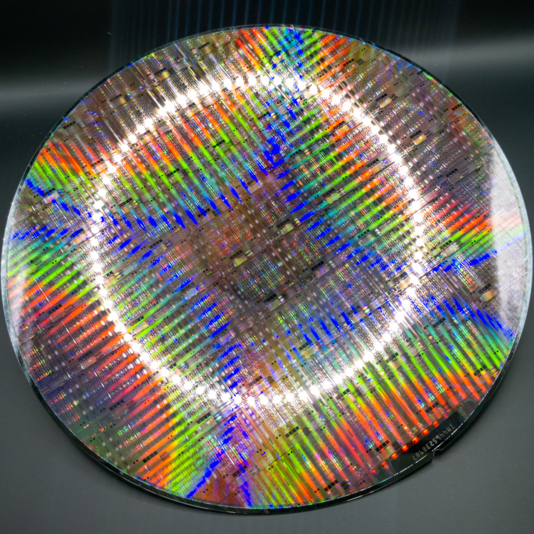
A 200 mm commercial 3rd party wafer that has been post-processed with plasmonic structures, and a non-linear material subject to the Pockels effect for efficient modulation of light.
Plasmonics Fits to Virtually any SiPh Process and PDK

Silicon photonics layer stack, in-plane plasmonic slot and integration dielectric and interconnect layers (photonic coupling not shown).

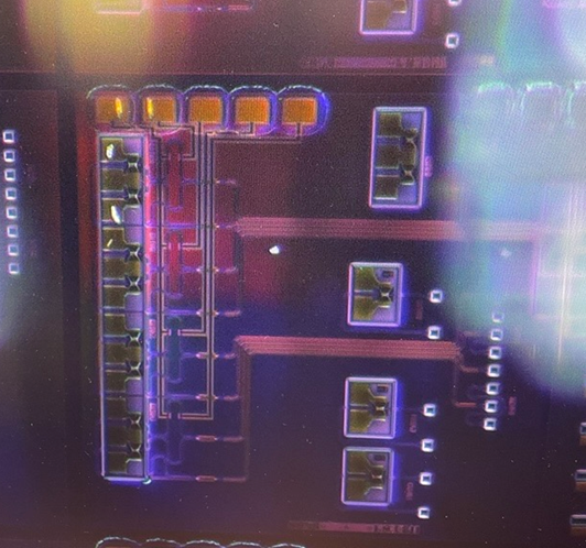
Plasmonic 3rd-party silicon photonics wafer-level integration.
Integrating plasmonic modulators into 3rd-party silicon photonics workflow is surprisingly straightforward! Initial cycle times as low as 3 months, and subsequent can be sped up as required. Thanks to backend processing, Polariton can seamlessly add these high-performance components without disrupting established front-end fabrication. This compatibility extends to a wide array of silicon photonics processes, making it a truly versatile upgrade. The result? A significant leap in performance, unlocking new possibilities for your integrated photonics.
The backend process, requiring certain CMOS incompatible materials, is performed in a selected set of commercial foundries and according to the customer’s expectation. Organic integration is followed by hermetic sealing to protect from the environment and unleash the reliability of our PICs.