Neural Intelligence Done with Light
Optical signals degrade as they travel through fiber, requiring complex electronic equalization to restore data integrity. These traditional digital-signal-processing steps have become increasingly demanding because of high-speed applications, consuming significant power and adding both latency and hardware overhead to modern transceivers. As data centers and AI platforms scale their infrastructure and performance, processing steps are turning from electronic to optic.
Researchers from ETH Zurich’s Department of Information Technology and Electrical Engineering (D-ITET), in collaboration with the Aristotle University of Thessaloniki and Polariton Technologies AG, have now demonstrated a fundamentally different solution: a photonic/plasmonic artificial neural network that performs key signal-processing tasks directly in light.
This marks an important step toward high-speed, low-power, next-generation optical systems — and toward a new era where photonic integrated circuits (PICs) carry not only information, but also part of the intelligence needed to process it.
Replacing Complex Electronic Processing With Light
The work, published in Science Advances under the title “Digital and Plasmonic Artificial Neural Networks – Improved Nonlinear Signal Processing at High Speed and Low Complexity”, presents a hybrid neural-network architecture that merges digitally trained intelligence with an ultrafast plasmonic chip.
“Put simply, we bring part of the ‘intelligence’ directly to the plasmonic chip instead of performing complex calculations in the electronics,” explains first author Tobias Blatter from ETH Zurich’s Institute of Electromagnetic Fields (IEF). By doing so, the researchers achieved highly efficient equalisation of distorted optical signals, but with a fraction of the energy and hardware traditionally required.
Prof. Juerg Leuthold, who supervised the work, emphasises the magnitude of this step: “This chip has the potential to replace decades of traditional signal-processing technology, reducing hundreds to thousands of electronic operations to just a few dozen optical ones.”
This overturns the common belief that neural-network technologies inevitably increase energy consumption. Instead, this demonstration shows that photonic neural networks can reduce it.

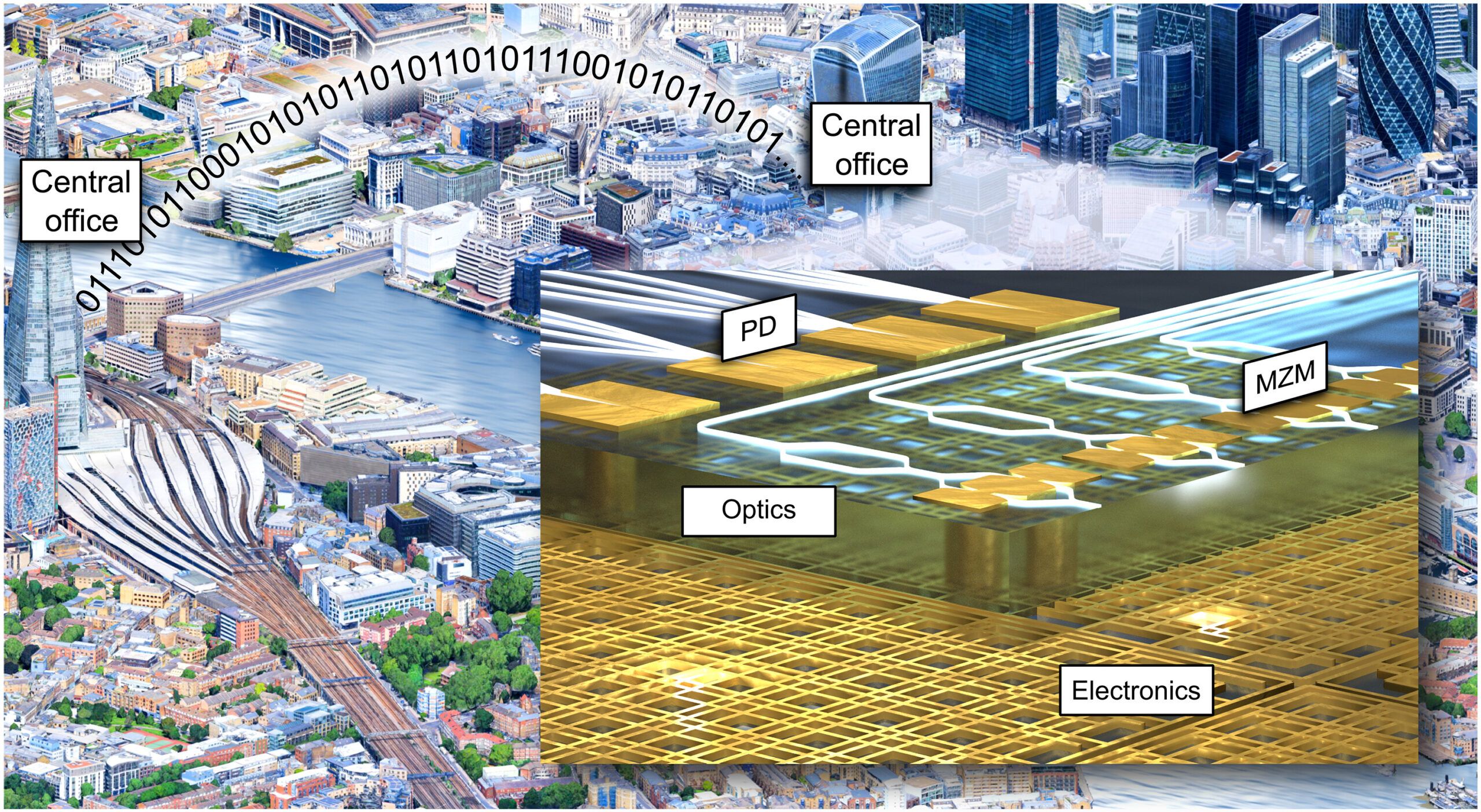
Fig. 1. Device and application. the image illustrates two connected transceivers in central offices. in the central offices, receivers relying on plasmonic ANNs may directly process optical signals independent of the bandwidth. the concept is shown in the inset: the chip consists of a photonic and an electronic layer stack. the pho-tonic stack hosts the optical MAc schemes and highspeed, ultracompact plasmonic modulators. the electronic stack hosts some of the nonlinear activation functions and is needed to control the linear operations in the optical stack. Also, it serves as an electronic data interface to the chip. (Taken from original publication)
Why This Matters for Users: Faster, Simpler, More Efficient Systems
For system designers, especially in data centers, AI computing, and high-performance interconnects, reducing electronic processing is a clear benefit.
Polariton’s COO, Wolfgang Heni, highlights exactly why: “Embedding neural-network functionality directly in photonic hardware reduces electronic processing and enables faster, more energy-efficient systems. This breakthrough in photonic neural-network technology opens new possibilities for data centers, AI platforms, and high-performance computing.”
In environments where every watt counts, and where growing data flows demand more bandwidth and lower latency, solutions that compute in light rather than electrons can meaningfully reshape system architecture.
Behind All This? Plasmonics
Plasmonic modulators are uniquely suited for this kind of application thanks to their small footprint, broadband operation, and ultrafast response. Polariton contributed directly to this work by manufacturing the plasmonic modulator chips used in the demonstration and co-designing the components.
The chip’s tiny dimensions enable dense photonic integration, while its speed supports the extremely fast nonlinear transformations required by neural networks.
As Tobias Blatter explains: “What makes this system special is the combination of ultra-compact plasmonic hardware, genuine nonlinear signal processing directly on the chip, and a simple network that is nevertheless surprisingly powerful at reversing distortions.”
This combination enables new architectures that were previously unattainable with photonics alone.
Implications Beyond Equalisation
The demonstrated photonic neural network equalised high-speed optical signals, but its potential applications extend much further:
-
optical transceivers in data centers,
-
AI and HPC interconnects,
-
short-reach and long-reach optical links, and
-
specialized AI accelerators that compute using light instead of electrons.
This may open the door to low-power AI pre-processing at the physical layer, a direction that aligns strongly with next-generation photonic system needs.
Read More
Full article in Science Advances: https://www.science.org/doi/epdf/10.1126/sciadv.adx1657
Congratulations and thanks to all authors and collaborators, especially the teams at ETH Zurich and AUTH, for advancing this important work.