
Plasmonic phase modulator consisting of a metal-insulator-metal waveguide and an electro-optic material in the slot.
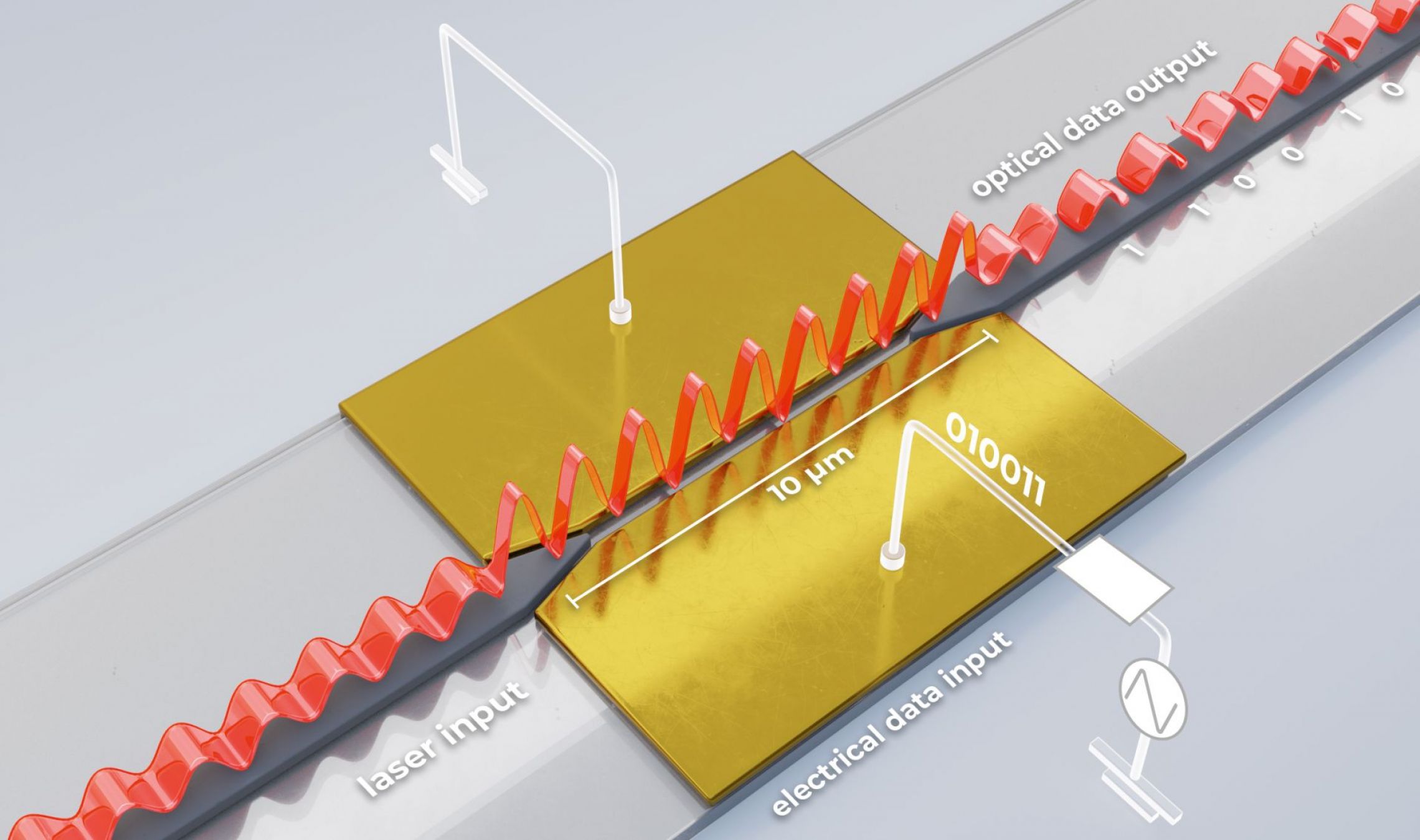
Plasmonics refers to the manipulation of signals at optical frequencies along metal-dielectric interfaces at the nanometer scale. Key to this technology is the coupling between light and the electrons at the metal surface, called surface plasmon polaritons (SPP). Similarly in such structures, these SPPs are strongly confined in a metal-insulator-metal (MIM) waveguide, where they interact with the electro-optic material in the slot. Then, when a voltage is applied across the electrodes, the optical property of the electro-optic material changes the phase of the SPPs, having an effect on the path length of the optical wave. Basically, this configuration permits the construction of highly effective phase shift modulators (PSM).
Because, the mentioned tight confinement works at the micrometer scale, it provides a breakthrough in terms of footprint, orders of magnitude smaller than photonic technologies. Consequently, a phase shifter can be implemented as small as 10 µm in length, having a positive effect on the photonic losses.
Plasmonic devices use the metal of the MIM waveguide as their own electrical contact, hence, allowing for small capacitances that ultimately boost the switching speed thanks to small RC time constants. Further, in contrast to photonic structures, plasmonic devices do not experience a spatial walk-off of the optical wave which would reduce modulation efficiency.
Finally, the advantage of small structures in electronics is the reduced power dissipation, of at least one order of magnitude. Since plasmonic structures can be implemented as lumped high-impedance devices, transmission-line effects can be ignored, and further power dissipation reduction is possible when driven with a high-impedance, high-speed driver circuit. Given these points, plasmonics is a key to next-generation signal transmission in the THz regime.
Plasmon: a quantum of plasma oscillation is the equivalent quasiparticle to phonons (quantizations of mechanical vibrations).
Surface plasmon: a coherent delocalized electron oscillation. Such plasmons reside at a metal-dielectric interface where they strongly interact with light, forming a polariton.
Polariton: a quasiparticle consisting of an electromagnetic wave that is strongly coupled to an electric or magnetic dipole-carrying excitation. The polariton is a bosonic quasiparticle.
Surface plasmon polariton (SPP): an electromagnetic excitation existing at a metal-dielectric interface and thus a solution to Maxwell’s equations.


The SPP overcomes Abbe’s diffraction limit and allows control and manipulation of the propagation and dispersion of light on the micro- or nanometer scale.
In a silicon waveguide, the incident wave has a photon momentum of:


Figure 1a: Schematic illustration of an SPP electromagnetic wave and surface charges at the metal-dielectric interface.

Figure 1b: Local electric field as a function of distance to the interface.
the refractive index of silicon and the free space wavelength of the incident light.
Upon entering a metal-dielectric-metal slot, the SPP dispersion relation can be determined by Maxwell’s equation as
![\[ k_{\text{SPP}} = k \sqrt{\frac{\varepsilon_d \cdot \varepsilon_m}{\varepsilon_d + \varepsilon_m}} = \frac{ 2\pin_S_i}{\lambda} \hspace{1cm} (2) \]](https://www.polariton.ch/wp-content/ql-cache/quicklatex.com-4764fef7d00dbe1f0283c9be8c072dca_l3.png "Rendered by QuickLaTeX.com")
with
![\[ k,{\varepsilon_d,_m , {\lambda} _S_P_P \]](https://www.polariton.ch/wp-content/ql-cache/quicklatex.com-b5d935ffa5833da92b7f11d2dc775114_l3.png "Rendered by QuickLaTeX.com")
the free-space wave vector, the dielectric and metal permittivity and the effective wavelength of the SPP (Figure 1a). The electromagnetic field is enhanced at the surface and decays exponentially away from the interface (Figure 1b). Subsequently, a full derivation of the equations can be found in [1]. The SPP gradually attenuates due to losses from absorption in the metal. The propagation length depends on the dielectric constant of the metal as well as the incident wavelength.
Plasmonics refers to the manipulation of signals at optical frequencies along metal-insulator-metal (MIM) interfaces at the nanometer scale.
In a plasmonic phase shifter, light from a continuous-wave laser source is guided into the slot that is narrower than the wavelength, thus forming an SPP. Thereafter, gold electrodes serve as waveguides (light field) as well as electrical contacts (electrical field). The SPP propagates along the slot filled with a non-centrosymmetric material exhibiting high second-order optical non-linearity.
henceforth, There is a range of different materials suitable for these applications. Prominent examples are Barium Titanate (BTO) for plasmonics in the visible and infrared, and organic polymers as a versatile class of materials with excellent performance tailored to a specific application and facile deposition. As many materials, these require careful protection from the environment. Continuous research will further broaden the library of available non-linear materials.
A voltage is applied to these metallic waveguides to manipulate the light leading to a voltage drop across nonlinear material [2]. The instantaneous Pockels effect results in a change in the refractive index (see equation 2) and thus a phase shift of the propagating SPP compared to the SPP at zero applied voltage. In this way, the pulsed voltage signal is translated into a modulated laser output signal.
The surface plasmon polariton inside the slot has quasi-TE polarization perpendicular to the slot direction and parallel to the wafer surface. Modulation of other polarizations can be achieved by rotating the light after the phase shifter.
To minimize plasmonic losses, the slot size can be reduced as well as the choice of active material and device geometry optimized. The benefits of employing plasmonics in photonic integrated circuits are the small footprint, ultra-high bandwidth, low power use and compatibility with the established Silicon Photonics platform.

Figure 2: High-speed plasmonic micro-RT modulator concept.

Figure 3: Schematic cross-section of a metallic slot on insulator filled with organic electro-optical material.
Small Dimensions
Plasmonics is characterized by the excellent overlap between the driving and optical fields (Figure 4, [3]) This results in efficient interactions even at short slot lengths of a few 10s of µm, effectively bridging the gap between the small scale of electronics and the larger scale of photonics.
Benefits
-
 Compatible size scales of electronics and photonics components.
 -
Integration of a larger number of active devices and enabling circuits of larger complexity.
-
Effective use of silicon wafer real estate.
![Figure 5_ Bandwidth measurement of plasmonic Mach-Zehnder modulator. [4]](https://www.polariton.ch/wp-json/yootheme/image?src=%7B%22file%22%3A%22wp-content%2Fuploads%2F2024%2F10%2FFigure-4_-Comparison-of-optical-E-field-and-driving-E-field-in-a-plasmonic-slot.-3-1-1.png%22%2C%22type%22%3A%22webp%2C100%22%2C%22thumbnail%22%3A%22700%2C700%2C%2Cleft%2Ccenter%22%7D&hash=51c83256)
Figure 4: Comparison of optical E field and driving E field in a plasmonic slot.
![Figure 5_ Bandwidth measurement of plasmonic Mach-Zehnder modulator. [4]](https://www.polariton.ch/wp-json/yootheme/image?src=%7B%22file%22%3A%22wp-content%2Fuploads%2F2024%2F10%2FFigure-4_-Comparison-of-optical-E-field-and-driving-E-field-in-a-plasmonic-slot.-3-2-1.png%22%2C%22type%22%3A%22webp%2C100%22%2C%22thumbnail%22%3A%22700%2C700%2C%2Cleft%2Ccenter%22%7D&hash=744c28e9)
Ultra-high Speed
The metal waveguides, which also function as electrodes, provide a distinct electro-optic bandwidth that extends into the millimeter-wave and THz ranges (up to 500 GHz, Figure 5, [4]) The device can operate in the O-E-S-C-L-U optical bands, with a current emphasis on the O, C and L bands.
Benefits
-
Enabling high-speed data transmission.
-
Operation in the sub-THz regime with simple schemes.
-
Flexibility and versatility in the optical bands.
![Figure 5_ Bandwidth measurement of plasmonic Mach-Zehnder modulator. [4]](https://www.polariton.ch/wp-json/yootheme/image?src=%7B%22file%22%3A%22wp-content%2Fuploads%2F2024%2F10%2FFigure-5_-Bandwidth-measurement-of-plasmonic-Mach-Zehnder-modulator.-4.png%22%2C%22type%22%3A%22webp%2C100%22%2C%22thumbnail%22%3A%22700%2C700%2C%2Cleft%2Ccenter%22%7D&hash=f44e7e6f)
Figure 5: Schematics of a dual-drive Mach Zehnder modulator
Energy Efficiency
Plasmonic devices do not have traveling wave electrodes, allowing for the application of a differential voltage drop. Further, the device’s lumped capacitance, which lacks a 50 Ohm termination, reduces the necessary voltage by half compared to conventional devices (Figure 6, [5]) Additionally, the high bandwidth of plasmonic devices reduces the need for power-intensive DSP and FEC at the system level.
Benefits
-
Reduced power consumption and improved energy efficiency.
-
Reduced need for signal processing due to high bandwidths.

Figure 6: Bandwidth measurement of plasmonic Mach-Zehnder modulator
Scalability
Plasmonic devices can be added to the silicon photonics platform and thus permit seamless integration into an already mature technology (Figure 7, [6]) Since these two platforms are supported by several high-volume manufacturing companies, we foresee a growing adoption in various formats and architectures.
Benefits
-
Scaling path to high volume production.
-
Industry leading cycle times.
-
Large choice of compatible 3rd party PDKs.
![Figure 7_ Design layout for monolithic photonic integrated circuit for high-speed transmission. [6]](https://www.polariton.ch/wp-json/yootheme/image?src=%7B%22file%22%3A%22wp-content%2Fuploads%2F2024%2F10%2FFigure-7_-Design-layout-for-monolithic-photonic-integrated-circuit-for-high-speed-transmission.-6.png%22%2C%22type%22%3A%22webp%2C100%22%2C%22thumbnail%22%3A%22700%2C700%2C%2Cleft%2Ccenter%22%7D&hash=2c745e24)
Figure 7: Design layout for monolithic photonic integrated circuit for high-speed transmission
Plasmonic Losses
Optical insertion losses are higher for plasmonic phase shifters, the simplest building block, compared to photonic electro-optical modulators. Values are proportional to the slot length and can thus be tailored in a limited range.
The architecture of the Resonant Ring Modulator shows significantly lower insertion losses, since only a part of the beam is coupled into the ring. In addition, continuous improvement of design and manufacturing processes reduces the amount of losses caused by passive building blocks and fabrication impurities. Encapsulation of the electro-optic polymer leads to greater stability for long operation times. Ask us for the loss values of the newest generation modulators!


Small Dimensions
Plasmonics offers dense integration with sizes of a few 10s µm. This overcomes the size mismatch between small-scale electronics and large-scale photonics.
Features
-
On-chip device sizes of a few 10s of µm
-
Package sizes of 20 mm x 10 mm
-
Minimize RF losses and attach directly to RF source


Large Bandwidth
Thanks to small RC time constants plasmonic devices offer a unique electro-optic bandwidth well into the THz regime.
Features
-
Demonstrated on-chip bandwidth of up to 500 GHz
-
Capable of operation in O-E-S-C-L-U optical bands


Low Power
The power consumption in fiber-optic communication networks strongly depends on the system design that requires new and highly efficient components. The high bandwidth of plasmonic devices minimizes the need of power-hungry DSP and FEC needs on a system level.
